Generic placeholder image

Nanoscience & Nanotechnology-Asia

Editor-in-Chief

ISSN (Print): 2210-6812
ISSN (Online): 2210-6820

Research Article

Sol-gel Growth of Ni-doped CdS on Glass Substrates: Effect of Spin Coating Speed and Dopant Concentration

Author(s): Atefeh N. Setayesh* and Hassan Sedghi

Volume 11, Issue 2, 2021

Published on: 23 April, 2020

Page: [230 - 236] Pages: 7

DOI: 10.2174/2210681210999200423120817

Price: $65

Abstract

Background: In this work, CdS thin films were synthesized by the sol-gel method (spin coating technique) on glass substrates to investigate the optical behavior of the film.

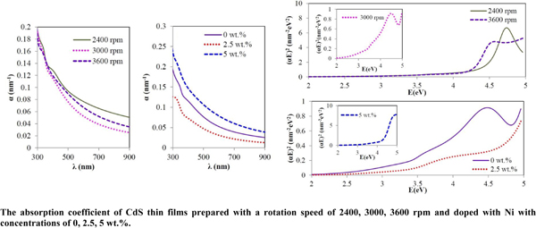
Methods: Different substrate spin coating speeds of 2400, 3000, 3600 rpm and different Ni dopant concentrations of 0 wt.%, 2.5 wt.%, and 5 wt.%) were investigated. The optical properties of thin films, such as the refraction index, extinction coefficient, dielectric constant, and optical bandgap energy of the layers were discussed using spectroscopic ellipsometry method in the wavelength range of 300 to 900 nm.

Results: It can be deduced that substrate rotation speed and dopant concentration have an influence on the optical properties of thin films by decreasing the rotation speed of the substrate, which results in films with more thicknesses, and more optical interferences were observed in the results.

Conclusion: The samples doped with Ni, when compared to pure ones, were found to have more optical bandgap energy.

Keywords: CdS, thin film, sol-gel, spectroscopic ellipsometry, Ni dopant, spin coating speed.

Graphical Abstract
[1]
Pushpalatha, H.L.; Bellappa, S.; Narayanawamy, T.N.; Ganesha, R. Structural and optical properties of CdS thin film obtained by chemical bath deposition and effect of annealing. Indian J. Pure Appl. Phy., 2014, 52, 545-549.
[2]
Kamal, T.; Parvez, S.; Khabir, K.M.; Matin, R.; Hossain, T.; Sarwar, H.; Bashar, M.S.; Rashid, M.J. Chemical bath deposition of CdS layer for thin film solar cell. South Asian J. Res. Eng. Sci. Technol., 2017, 02, 610-617.
[3]
Guo, Y.; Jiang, J.; Zuo, S.; Shi, F.; Tao, J.; Hu, Z.; Hu, X.; Hu, G.; Yang, P.; Chu, J. RF sputtered CdS films as independent or buffered electron transport layer for efficient planar perovskite solar cell. Sol. Energy Mater. Sol. Cells, 2018, 178, 186-192.
[http://dx.doi.org/10.1016/j.solmat.2018.01.017]
[4]
Nobari, N.; Behboudnia, M.; Maleki, R. Systematics in morphological, structural and optoelectrical properties of nanocrystalline CdS thin films grown by electrodeposition method. Mater. Sci. Eng. B, 2017, 224, 181-189.
[http://dx.doi.org/10.1016/j.mseb.2017.08.002]
[5]
Shaikh, S.U.; Desale, D.J.; Siddiqui, F.Y.; Ghosh, A.; Birajadar, R.B.; Ghule, A.V.; Sharma, R. Effects of air annealing on CdS quantum dots thin film grown at room temperature by CBD technique intended for photosensor applications. Mater. Res. Bull., 2012, 47, 3440-3444.
[http://dx.doi.org/10.1016/j.materresbull.2012.07.009]
[6]
Chtouki, T.; El Kouari, Y.; Kulyk, B.; Louardi, A.; Rmili, A.; Erguig, H.; Elidrissi, B.; Soumahoro, L.; Sahraoui, B. Spin-coated nickel doped cadmium sulfide thin films for third harmonic generation applications. J. Alloys Compd., 2017, 696, 1292-1297.
[http://dx.doi.org/10.1016/j.jallcom.2016.12.089]
[7]
M. M. ShahidKhan. A. Aziz, S. A. Rahman, Z. RazaKhan. Spectroscopic studies of sol–gel grown CdS nanocrystalline thin films for optoelectronic devices Mater. Sci. Semicond. Proc., 2013, 16, 1894-1898.
[8]
Oliva, A.I.; Corona, J.E.R. Patiño And A. I. Oliva-Avilés, Chemical bath deposition of CdS thin films doped with Zn and Cu. Bull. Mater. Sci., 2014, 37, 247-255.
[http://dx.doi.org/10.1007/s12034-014-0642-9]
[9]
Sonawane Shivaji, M. Characterization of CdS Thin Film Grown by Chemical Bath Deposition Int. Res. J. Sci. Eng. A, 2018, 2, 221-224.
[10]
Kumar, S.; Sharma, J.K. Effect of nickel doping on optical properties of CdS nanoparticles synthesized via. Co-precipitation Technique. Mater. Sci. Res. India, 2017, 14, 05-08.
[11]
Abdolahzadeh Ziabari, A.; Ghodsi, F.E., Growth, characterization and studying of sol–gel derived CdS nanoscrystalline thin films incorporated in polyethyleneglycol: Effects of post-heat treatment. Sol. Energy Mater. Sol. Cells, 2012, 105, 249-262.
[http://dx.doi.org/10.1016/j.solmat.2012.05.014]
[12]
Abdolahzadeh Ziabari, A.; Ghodsi, F.E. Influence of Cu doping and post heat treatment on the microstructure, optical properties and photoluminescence features of sol–gel derived nanostructured CdS thin films. J. Luminescence, 2013, 141, 121-129.
[13]
Bairy, R.; Jayarama, A.; Shivakumar, G.K.; Kulkarni, S.D.; Maidur, S.R.; Patil, P.S. Effect of Aluminium doping on photoluminescence and third-order nonlinear optical properties of nanostructured CdS thin films for photonic device applications. Phys. B Phys. Conden. Matter., 2018, 555, 145-151.
[http://dx.doi.org/10.1016/j.physb.2018.11.054]
[14]
Shaban, M.; Mustafa, M.; El Sayed, A.M. Structural, optical, and photocatalytic properties of the spray deposited nanoporous CdS thin films; influence of copper doping, annealing, and deposition parameters. Mater. Sci. Semicond. Process., 2016, 56, 329-343.
[http://dx.doi.org/10.1016/j.mssp.2016.09.006]
[15]
Ouafi, M.; Jaber, B.; Laânab, L. Low temperature CBD growth of CdS on flexible substrates: Structural and optical characterization. Superlattices Microstruct., 2019, 129, 212-219.
[http://dx.doi.org/10.1016/j.spmi.2019.03.024]
[16]
Tanushevski, A.; Osmani, H. CdS thin films obtained by chemical bath deposition in presence of fluorine and the effect of annealing on their properties. Chalcogenide Lett., 2018, 15, 107-113.
[17]
Al-Jawad, S.M.H. Comparative study between CBD and SILAR methods for deposited TiO2, CdS, and TiO2/CdS core-shell structure. Mater. Sci. Semicond. Process., 2017, 67, 75-83.
[http://dx.doi.org/10.1016/j.mssp.2017.05.014]
[18]
Ibrahim, N.B.S.M. AL-Shomar, S. H. Ahmad, Effect of aging time on the optical, structural and photoluminescence properties of nanocrystalline ZnO films prepared by a sol–gel method. Appl. Surf. Sci., 2013, 283, 599-602.
[http://dx.doi.org/10.1016/j.apsusc.2013.06.155]
[19]
Fricke, L.; Bontgen, T.; Lorbeer, J.; Bundesmann, C.; Grund, R.S.; Grundmann, M. An extended Drude model for the in-situ spectroscopic ellipsometry analysis of ZnO thin layers and surface modifications. Thin Solid Films, 2014, 571, 437-441.
[http://dx.doi.org/10.1016/j.tsf.2014.02.010]
[20]
Galvan, A.M.; Cruz, C.T.; Lee, J.; Bhattacharyya, D.; Metson, J.; Evans, P.J.; Pal, U. Effect of metal-ion doping on the optical properties of nanocrystalline ZnO thin films. J. Appl. Phys., 2006, 99, 014306.
[http://dx.doi.org/10.1063/1.2158503]
[21]
Leng, J.; Opsal, J.; Chu, H.; Senko, M.; Aspnes, D.E. Analytic representations of the dielectric functions of materials for device and structural modeling. Thin Solid Films, 1998, 313-314, 132-136.
[http://dx.doi.org/10.1016/S0040-6090(97)00799-2]
[22]
Peters, S. spectra ray and application tutorial, Spectroscopic ellipsometry-theory and application 2009.
[23]
Motallebi Aghgonbad, M.; Sedghi, H. Spectroscopic ellipsometry studies on zinc oxide thin films deposited by sol–gel method with various precursor concentrations. Surface Rev. Lett., 2018, 2018, 1850158.
[http://dx.doi.org/10.1142/S0218625X18501585]
[24]
Tauc, J.; Grigorovici, R.; Vancu, A. Optical properties and electronic structure of amorphous germanium. Phys. Stat. Sol., 1966, 15, 627-637.
[http://dx.doi.org/10.1002/pssb.19660150224]
[25]
Khan, Z.R.; Munirah, A. Aziz, M.S. Khan, Sol-gel derived CdS nanocrystalline thin films: Optical and photoconduction properties. Mater. Sci. Pol., 2018, 36, 235-241.
[http://dx.doi.org/10.1515/msp-2018-0028]
[26]
Thambidurai, M.; Murugan, N.; Muthukumarasamy, N.; Vasantha, S.; Balasundaraprabhu, R.; Agilan, S. Preparation and characterization of nanocrystalline CdS thin films. Chalcogenide Lett., 2009, 6, 171-179.
[27]
Olopade, M.A.; Awobode, A.M.; Awe, O.E.; Imalerio, T.I. Structural and optical characteristics of sol-gel spin-coated nanocrystalline CdS thin film. IJRRAS, 2013, 15, 120-124.
[28]
Dissanayake, D.M.C.U.; Samarasekara, P. Optical and structural properties of spin coated cadmium sulfide thin films. J. Sci. Univ. Kelaniya, 2015, 10, 13-20.
[http://dx.doi.org/10.4038/josuk.v10i0.7989]

Rights & Permissions Print Cite
© 2024 Bentham Science Publishers | Privacy Policy